What a PCB Inspection Microscope Can Reveal—and What It Cannot
- li
- 545 reads
Microscopes clarify exposed PCB and solder features, but hidden joints and internal connections need other inspection methods.
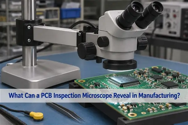
A PCB inspection microscope is most useful when an engineer needs to resolve a specific visible feature: a suspected trace nick, solder bridge, lifted lead or particle near a pad. It can provide a close view and a record of that location. It cannot see through a BGA package, establish the integrity of a buried connection or prove that a joint conducts electricity.
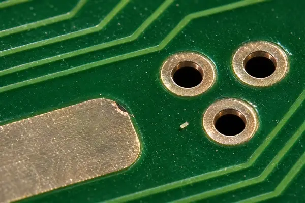
That boundary is the practical starting point. The drawing, suspected defect, viewing angle, lighting and acceptance requirement determine what an image can establish. Magnification helps gather evidence; it does not set the pass or fail criterion. Automated optical inspection (AOI), electrical testing, X-ray and microsection imaging each answer different questions.
What magnified viewing can show
Stereo microscopes use separate viewing paths to provide depth cues, while digital systems show an image on a screen and can capture it for review. Both rely on a clear line of sight. On a bare board, they can help inspect exposed copper features, solder-mask edges, pads, plated-hole entrances and surface particles. On an assembled board, they can show accessible lead alignment, visible solder fillets, bridges and displaced small parts.
Start with a wider view to identify the board area, component and orientation. Then increase magnification until the feature is clear, keeping enough context to locate the close-up again. At very high magnification, the field of view shrinks and depth of field decreases. Nearby pins may disappear from view, and a shadow or reflection can look like a defect.
For bare boards, a close view may clarify whether an apparent trace nick is real, whether solder mask reaches the pad edge, or whether a particle is present. It can also show the accessible entrance of a plated hole. But an image of that entrance cannot establish copper thickness or continuity deeper in the barrel. Likewise, on a fine-feature HDI board, seeing a suspected nick beside a microvia land does not reveal the buried connection. Electrical testing or a prepared microsection may be needed for those questions.
On a PCB assembly, a stereo view can help assess exposed lead-to-pad alignment and the shape or height of a visible fillet. Interpretation still depends on package geometry and the assembly requirement. A dark line between pins could be a shadow; a bright line could be reflected light. Change the viewing or lighting angle before treating either as a defect. A good-looking fillet also says nothing conclusive about a hidden interface beneath a bottom-terminated package.
Match the method to the inspection question
Microscope inspection works well as a targeted follow-up: for example, after an AOI flag, an ambiguous incoming-board finding, local rework or a failure investigation. AOI can screen visible features repeatably; magnified review can clarify an individual location; electrical test checks specified connections; and a prepared cross-section exposes internal construction. No single method covers all four jobs.
| Inspection question | What magnified viewing can establish | What may be needed next |
|---|---|---|
| Are two exposed leads joined by solder? | A clear view of the named lead gap can show a visible bridge. | Compare with the circuit netlist and use an appropriate electrical check before calling it an unintended short. |
| Is there a particle near exposed pads? | It can locate and image the particle. | Separate analysis may be needed to identify the material or assess a cleanliness concern. |
| Is a plated hole sound through the board? | It can show the accessible hole entrance. | Use electrical testing and, if internal construction is in question, an approved microsection. |
| Are hidden BGA balls joined correctly? | It cannot see the concealed interfaces. | Use suitable X-ray inspection and electrical or functional testing for the suspected failure mode. |
The dividing line is access. When the feature is exposed, a microscope may settle a visual question. When the feature is inside the board or beneath a package, more zoom cannot restore the missing line of sight. Naming the feature and concern before requesting images helps determine which inspection stage can produce useful evidence.
Magnification, optics and lighting
Leica describes roughly 5x to 30x as a practical range for general PCB inspection with stereo or digital systems: around 5x for board-area orientation and approximately 25x to 30x for finer surface detail. That range is an application guideline, not a universal IPC acceptance magnification or a specification for any particular inspection station.
Useful detail depends on more than the number printed on a microscope. Optical resolution, camera sampling, focus and illumination all affect what the system can distinguish. A large digital zoom figure does not guarantee that adjacent features will resolve clearly. A formal judgment should use the magnification and criteria specified by the applicable work instruction or acceptance standard.
Lighting changes contrast, especially on reflective solder. A ring light can illuminate a broad area, but direct reflections may hide a fillet’s contour. Diffused or oblique light can expose an edge or particle that was hard to distinguish under direct illumination. Viewing angle matters too: a near-vertical view helps locate a feature among pads, while a side view can clarify the profile of a raised lead or exposed fillet. Tall components, shields and connectors can block the view altogether. Leica’s inspection examples show how changing illumination can reveal different PCB details, including holes and recesses.
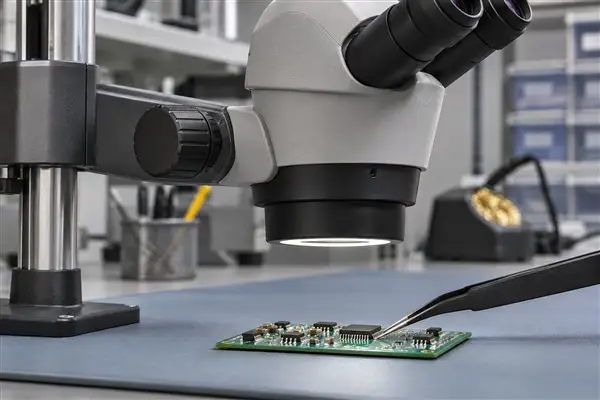
One published equipment example, the Leica A60 H, shows how the rest of the optical setup affects inspection. These are manufacturer specifications for that microscope, not universal acceptance requirements:
| Parameter | Leica A60 H published value | Inspection effect |
|---|---|---|
| Zoom range | 8x-48x | Supports area orientation and closer surface review on the same instrument. |
| Maximum object field | 30 mm | Sets how much of the board is visible at the low end of the zoom range. |
| Working distance | 122 mm without illumination | Provides room for the board and, where appropriate, a probe or rework tool; an illuminator can affect clearance. |
| Maximum depth of field | 10.3 mm | Helps keep features at different heights in focus at the relevant low-zoom setting; depth of field varies with zoom. |
| Illumination | LED ring light with removable diffuser | Allows a more diffuse view of reflective surfaces. |
The Leica A60 H brochure gives 8x a 30 mm object field and up to 10.3 mm depth of field; at 20x, the field is 12 mm and depth of field is 2 mm. The useful setting is therefore the one that keeps the target identifiable, in focus and correctly located—not simply the highest available zoom. For dimensional evidence, add a calibrated scale or reticle, a stated measurement method and a clear definition of the feature. Nominal magnification alone cannot support a reported trace width or defect dimension.
Stereo or digital: choose for the workflow
Stereo viewing suits tasks where depth perception and hands-on access matter, such as assessing an exposed lead or repositioning a board. Digital viewing makes it easier to show the same image to several reviewers, save it and annotate it. Neither system can reveal a joint hidden by a package.
| Task | Stereo viewing | Digital viewing |
|---|---|---|
| Assess exposed lead height or fillet shape | Binocular depth cues help interpret height. | May require additional angles or focus changes to communicate depth. |
| Share a suspected defect | A camera attachment or separate capture method is needed for a common image. | Screen capture can simplify joint review and annotation. |
| Move around a tall assembled board | Check stand reach and working distance with the actual board. | Check camera clearance, stand reach and display latency with the actual board. |
| Inspect hidden BGA balls | Not visible through the package. | Not visible through the package. |
A stereo microscope with a camera can support both close examination and documentation. A digital capture workflow may suit repeatable photo review across a team. The choice depends on resolution, lighting, board size, access and record requirements—not on the label “digital” or advertised maximum zoom alone.
Investigating a suspected solder bridge
Consider adjacent leads on a small-outline IC that appear joined in an AOI image. First identify the component, board side and named pins using the assembly drawing and board orientation. At low magnification, keep the component marking and suspect side in view. Then increase magnification only enough to inspect the gap between those leads.
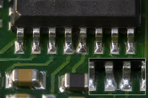
Change the light or viewing angle. If a bright line moves with the reflection while the physical gap remains visible, the first image did not establish a bridge. If metal appears continuous between the named leads from more than one useful angle, record the location and image before rework. One close-up does not establish the condition of every other pin.
Disposition depends on the observation and the assembly requirement. A visible connection may call for controlled rework followed by repeat inspection; an ambiguous finding may call for another view. Electrical continuity can help investigate the concern, but the circuit may contain legitimate connections elsewhere. Compare the measurement with the approved schematic or netlist before identifying an unintended short.
A useful record for this case includes the component and pins, board side, an orientation image, a close-up under stated lighting, the disposition and any post-rework check. That context lets another engineer revisit the same physical question instead of trying to infer it from a cropped image.
Hidden joints and inspection limits
A conventional optical microscope cannot see through a BGA package to judge its solder-ball interfaces. It may show a package edge, adjacent contamination or an exposed corner, but a clean edge view does not prove that the hidden balls are connected.
When the concern involves concealed joints, define suitable X-ray inspection and electrical or functional testing for the product and suspected failure mode. X-ray can show selected internal geometry and defects, but its image still requires interpretation and may not resolve every failure mode. A surface close-up is not a substitute for evidence about hidden joints.
The same principle applies after rework. A microscope can show whether accessible leads are aligned, whether a visible bridge is gone and whether nearby pads or parts appear damaged. Comparable before-and-after views are easier to review than unrelated close-ups. The inspection should cover adjacent features that may have been affected by heat or tool contact. A joint that looks acceptable may still have an electrical open, a damaged component or an intermittent connection, so the release record should name the additional check required by the approved process.
Making inspection records useful
Link each image to the board and requirement. Record the board revision, side, reference designator or coordinate, feature of concern, viewing direction, actual magnification or scale method, illumination and applicable acceptance document. Keep an orientation view alongside a close-up when the detail alone does not identify its location.
For a dimensional claim, include calibration or scale evidence and the measurement endpoints. For a qualitative finding, state what is visible and what remains unverified. IPC’s inspection-training syllabus distinguishes optical, automated and X-ray methods and calls for appropriate magnification and measurement-tool calibration; a photograph by itself is not a universal pass or fail standard.
What to specify in an inspection request
Describe the feature and the decision needed rather than writing only “inspect under microscope.” Identify the component or board coordinate, suspected condition, drawing revision, acceptance document and whether the request is for a photograph, measurement, rework decision or failure analysis. A prototype with one suspect pad needs a different record from routine lot screening.
Before production, agree on coverage and output: every unit or a defined sample, the sides and locations to inspect, the images or measurements to return, and the finding that triggers a hold or engineering review. If the concern is a hidden feature or internal hole wall, specify X-ray, electrical testing or microsection work rather than asking a surface image to answer it.
Provide the relevant drawing, Gerber or ODB++ data, BOM and assembly drawing along with the inspection question. For a large board, confirm that the stand has enough reach and working distance for the actual panel, including edge clearance and nearby component height. Zoom range alone does not establish that the board will fit beneath the optics.
For dimensional inspection, request a calibrated scale and a stated measurement method. For a visual finding, specify the location and acceptance basis. The most useful microscope image is one that answers a defined question, shows where the feature sits on the board and makes clear what still needs another inspection method.