PCB Microetching: Controlling Copper Removal, Surface Preparation and Process Uniformity
- li
- 486 reads
PCB microetching prepares exposed copper for later processing, but removal must be measured across the process route to protect conductor dimensions and interfaces.
PCB microetching sets up exposed copper for a later manufacturing step by dissolving a shallow surface layer. The process has to satisfy two requirements at once: prepare the copper for a resist, coating or plated metal, and preserve enough copper to meet the finished board’s thickness and geometry requirements. For fine conductors and thin copper, that allowance must be tracked across the full process route.
Surface preparation, not circuit formation
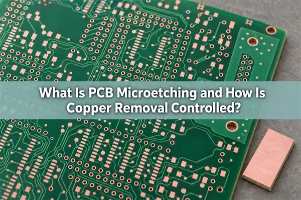
A microetch chemically dissolves the outermost copper. Depending on the chemistry, it can also produce a microscopic texture that helps a subsequent coating or deposited metal attach. The terms “microetching,” “micro etching” and “micro etch” refer to this surface preparation; they do not describe a small board or a method for forming the circuit pattern.
Pattern etching removes unwanted copper through the foil thickness to create traces and spaces. Microetching acts on exposed copper that generally needs to remain, so the controlled quantities differ: pattern etching affects conductor width, spacing and undercut, while microetching affects copper loss, surface condition and uniformity. A bright-looking surface by itself can’t establish that either process has met its dimensional target.
Cleaning and degreasing remove oils and other process contamination. Desmear removes resin residue associated with drilling. Some proprietary formulations combine cleaning and microetching, but that doesn’t make every microetch bath a degreaser, and copper microetching alone doesn’t replace desmear.
Where the treatment fits
Microetching can be placed before photoresist application, selected plating operations or final surface finishing. The required copper condition depends on the next step: resist needs an appropriate surface for adhesion, deposited metal needs a sound interface, and final finishing requires prepared exposed copper.
These are possible locations in a process route, not a reason to repeat the treatment at every stage. A board’s masked areas, exposed pads and plated features may have different exposure histories. The manufacturing route has to account for the copper removed at each stage and still deliver the specified finished copper and conductor dimensions.
Commercial chemistries include stabilized sulfuric acid and hydrogen peroxide systems, persulfate-based systems, and proprietary surface-preparation formulations. Bath composition, dissolved copper, additives and process conditions affect removal. Formulations can also produce different surface morphologies at similar removal depths, so chemistry selection depends on the following operation, equipment and acceptable copper loss as well as the oxidizer involved.
Operating limits belong to the specific product and production line. A temperature or copper-loading value from one formulation can’t safely be assumed to apply to another. Production systems also require the handling, ventilation and waste-treatment controls specified for their chemistry; these mixtures aren’t general-purpose workshop cleaners.
Keep removal, rate and roughness distinct
No single copper-removal target suits every board. The treatment must prepare the surface while preserving the minimum required copper and feature dimensions. Thin starting copper has less room for repeated removal than thicker copper, which makes cumulative exposure part of the copper budget.
Three measurements are often confused. Removal depth, expressed in micrometers (µm), describes the average copper thickness dissolved during treatment. Etch rate, expressed in µm/min, describes removal per unit time under stated conditions. Surface roughness, described with a defined parameter such as Ra or Rz in µm, measures profile variation; it is not the amount of copper removed. Finished copper thickness is the copper remaining after the relevant manufacturing operations.
For example, a measured rate of 1 µm/min over 30 seconds predicts 0.5 µm removal only if the rate and conditions remain applicable throughout the exposure. This calculation isn’t a recommended process setting. A roughness measurement of 0.5 µm also doesn’t mean that 0.5 µm of copper was dissolved.
Measuring removal with a coupon
One way to estimate the average removal is to weigh a copper coupon before and after treatment. The prescribed rinsing, drying and conditioning steps need to be repeatable: residual water, removable contamination or a change in laminate moisture can distort a small mass difference.
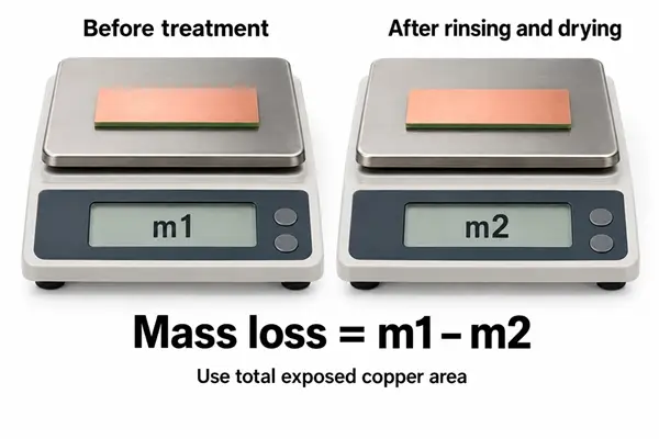
When the measured mass loss is copper, calculate average removal as follows:
Average removal (µm) = 10,000 × copper mass loss (g) / [copper density (g/cm³) × total exposed copper area (cm²)]
Average etch rate (µm/min) = average removal (µm) / exposure time (min)
Using a copper density of 8.96 g/cm³, a hypothetical loss of 0.0896 g over 100 cm² of exposed copper corresponds to 1 µm average removal. If exposure lasted one minute, the calculated average rate would be 1 µm/min. These figures demonstrate the calculation; they aren’t production test results.
Include every exposed copper surface in the area. Two coupon faces of 50 cm² each make 100 cm² total before any other exposed copper is counted. Using only one face would double the calculated depth. The coupon’s copper type, pretreatment and exposure should also represent the board process, since foil and plated copper may dissolve at different rates.
A coupon mass-loss result is an average across the measured area. It can’t establish the removal at a narrow trace edge or at the bottom of a blind microvia, where access and local flow may differ.
What shifts the result
Temperature and exposure time matter, but so do bath composition, dissolved copper, solution movement and the incoming copper condition. Conveyor speed sets a nominal dwell time; it doesn’t prove that each spray nozzle supplies the same flow or that every panel location receives equivalent treatment.
When measured removal changes, first check the measurement procedure: coupon area, timing, weighing and drying. Then compare bath temperature and chemistry analysis with the approved operating range. Review loading, replenishment history and the condition of incoming copper, followed by spray coverage or immersion circulation and panel placement. Repeat the measurement under controlled conditions, sampling different positions when needed.
Changing several variables at once makes the cause harder to identify. Extending dwell time may increase average removal while leaving a poorly supplied area inadequately prepared. A uniform average can therefore hide a local process problem.
Reading defects in context
Underetching can leave an unsuitable interface for the next operation. Overetching consumes copper that may be needed for thickness or conductor geometry. Neither condition can be confirmed from copper color alone. Poor adhesion may point to incoming cleanliness, preparation, coating application or cure; uneven appearance can reflect wetting, flow distribution, contamination or panel exposure. Excess coupon mass loss calls for checks of timing, area, temperature and bath analysis.
Narrow traces or thin finished copper require looking at accumulated removal across the route, not just the last bath. A plating-interface concern also involves activation and plating conditions. These observations narrow the investigation but don’t prove a microetch fault: contamination introduced after treatment, for example, can affect adhesion. Adding another microetch cycle without identifying the cause consumes more copper and may not resolve the defect.
Fine features and electrical performance
Fine-line designs and thin copper leave less room for unplanned removal. EBest Circuit’s stated HDI capability reaches line/space down to 2/2 mil on suitable constructions; the final stack-up, copper thickness and feature combination still need engineering review. That capability doesn’t define a universal microetch allowance.
Microvias add a local access problem. A flat coupon is easier for chemistry to reach than a recessed target pad, so solution exchange and preparation inside the feature need consideration for the actual geometry. Panel-surface measurements alone can’t demonstrate uniform treatment at the microvia target.
For impedance-controlled boards, finished conductor geometry affects impedance, while copper roughness can contribute to conductor loss at high frequency. Increasing roughness isn’t an unqualified improvement: preparation has to support the required interface while respecting the specified copper profile and electrical design.
Rinsing, verification and acceptance
Rinsing and transfer conditions influence both bath carryover and the state of prepared copper before the next operation. Whether the board moves wet-to-wet or is dried depends on the process that follows. Drying a coupon for weighing doesn’t establish that production boards should be dried at that point, and a transfer delay suitable for one resist or finish may not suit another.
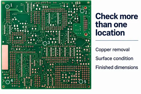
A useful quality check connects bath measurements to board results. Record the coupon type and exposed area, exposure time, bath condition, measurement method and panel position. Then assess the outcome relevant to the concern: remaining copper against the drawing, surface uniformity, adhesion or the plating interface. An average mass-loss result can’t answer all of those questions, and a passing thickness measurement doesn’t by itself settle an adhesion issue.
For manufacturing review, the stack-up, finished copper thickness, minimum line/space and surface-finish requirements give the process team the context needed to assess removal across the route. Special copper-profile or interface requirements matter too. The practical target is a repeatable surface preparation that supports the next operation while keeping finished board dimensions and copper within specification.
Common process questions
Can brushing replace chemical microetching?
Not without confirming the resulting surface condition, dimensions and compatibility with the next operation. Brushing acts mechanically on accessible surfaces; a chemical process acts on wetted copper. A brush also can’t reach every recessed feature.
Is microetching the same as black oxide treatment?
No. Microetching removes copper. Black oxide treatment produces a conversion layer used for bonding. An oxide-alternative process may include controlled etching, but its full chemistry and qualification can’t be inferred from the word “microetch.”
Does a microetch measurement prove the finished board is acceptable?
No. It describes one part of fabrication. Acceptance still depends on the specified dimensions, electrical tests, surface finish and other applicable product requirements.