PCB Layer Registration: Causes, Tolerances and Inspection Methods
- li
- 913 reads
Layer shifts can reduce via capture and clearance margins. Learn how fabrication controls alignment and what inspection methods can confirm.

Layer registration determines whether a drilled via lands on the copper features it is meant to connect, while preserving clearance from copper it must avoid. The practical risk is a margin problem: a hole can remain electrically connected yet leave too little copper around its barrel, or approach an internal plane closely enough to create an unintended connection. Controlling registration therefore means tracking both copper-to-copper alignment and drill position relative to the laminated stack.

Which registration measurement matters?
Layer-to-layer registration compares copper features on separate layers. Drill-to-copper registration compares a hole’s center with its pad or clearance. These measurements answer different questions: the first concerns overlap and spacing between layers; the second concerns hole capture and breakout. Solder-mask alignment concerns mask openings relative to surface pads, while component placement concerns assembly alignment. Neither tells you directly how well internal copper layers line up.
A tolerance is meaningful only when its datum and measurement method are clear. Measuring each layer against a common reference is different from reporting the largest separation between any two layers. A drawing that specifies one method cannot automatically be judged by another; the measured layer pair, features and panel locations need to match the stated requirement.
Where misalignment starts
Registration can change at several stages. Removing copper during inner-layer etching can alter a core’s dimensions. Temperature, moisture, material direction and prior processing also affect how materials move. During lay-up and bonding, incorrect orientation, worn tooling or movement under heat and pressure can add further error.
The spatial pattern can help narrow an investigation. Similar offsets at multiple targets may point to translation or a datum mismatch. An offset that changes direction across a panel may indicate rotation; one that grows with distance from the center may suggest a scale change. Local differences that remain after global alignment are consistent with nonuniform distortion. These patterns guide troubleshooting, but don’t identify a cause on their own. Moving the drilling origin may compensate for a uniform shift; it cannot undo local distortion already fixed into the bonded board.
| Observed pattern | Possible explanation to investigate | Useful comparison |
|---|---|---|
| Similar offset at several targets | Translation or datum mismatch | Target coordinates against the same origin |
| Offset changes direction across the panel | Rotation | Targets near opposite panel edges |
| Offset grows with distance from the center | Scale change | X and Y spans before and after processing |
| Different local errors remain after global alignment | Nonuniform distortion | Multiple targets across the usable panel |
How offset consumes annular-ring margin
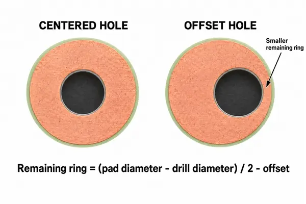
For circular geometry, a simple estimate of the narrowest remaining copper ring is:
Minimum remaining ring = (minimum pad diameter − maximum drilled-hole diameter) / 2 − center offset
Use dimensions from the same manufacturing stage. A finished plated-hole diameter is smaller than the drilled opening; using it in place of the drill diameter without accounting for plating can make the apparent margin too large.
For a 0.60 mm pad and a 0.30 mm drilled opening, ignoring diameter tolerances, a centered hole leaves 0.150 mm of ring. A 0.05 mm center offset reduces that to 0.100 mm; a 0.10 mm offset leaves 0.050 mm. At 0.15 mm, the hole and pad are geometrically tangent. These figures illustrate geometry, not acceptance limits. Pad etching, drill variation, layer movement and drilling position all use up available margin. A hole can also threaten an internal clearance even when its connected pad still captures it.
Write tolerances so they can be measured
There is no single registration tolerance that applies to every stack-up based only on layer count or a class designation. A fabrication drawing should identify whether a limit applies to layer-to-layer alignment, drill-to-pad position or a combined allowance. It should state whether the limit is radial or uses separate X and Y values, which targets and panel areas are checked, and whether the measurement is taken before bonding, after bonding or after drilling. The applicable specification revision, product class and drawing requirements also need to be agreed.
An X/Y limit is not automatically a radial limit. If each axis allows 0.05 mm, simultaneous displacement on both axes can produce a diagonal offset of about 0.071 mm. A drawing that intends a 0.05 mm radial maximum should say so explicitly.
Set the allowance against the smallest pad and clearance in the actual design. For Class 2 boards, assess layer registration against the applicable acceptance criteria and agreed fabrication requirements together. The geometric example above is not an IPC limit, and a class designation alone doesn’t define a positional tolerance.
Alignment through lay-up and bonding
Before lamination, optical registration equipment can locate etched targets and establish tooling holes relative to the copper artwork. This ties the tooling reference to the actual pattern instead of relying only on the laminate’s cut edge. Inner-layer AOI checks the etched pattern against design data while the copper remains visible. Correct core identity, orientation and sequence matter throughout lay-up: a well-aligned core installed in the wrong orientation is still misplaced.
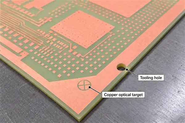
Tooling holes physically position material; optical targets provide a reference that equipment can locate and measure. They serve different purposes, and their geometry belongs to the board’s fabrication tooling plan. Copying target dimensions or positions from an unrelated design doesn’t establish a suitable reference for a new panel.
Bonding adds heat, pressure and resin flow, which can change the alignment set during loading. Dimensional compensation needs to account for the chosen laminate, copper distribution and process history rather than assume one scaling factor fits every job. Symmetric stack-ups and balanced copper distribution can help control dimensional behavior and warpage, but they don’t guarantee registration. Material orientation, compatible cores and prepregs, and bonding sequence also matter.
On an 8 layer PCB, checking target positions across all internal cores reveals more than inspecting only the outer layers. A proposed stack-up is a starting point; the approved materials and panel arrangement determine the fabrication route. Sequentially bonded structures need particular attention to movement accumulated across multiple bonding cycles.
What X-ray and other checks can show
After bonding hides the inner copper, X-ray inspection can locate suitable internal reference features and compare their positions. It can also help select drilling references. Measurement quality depends on the targets being distinguishable: overlapping features, unsuitable geometry or insufficient resolution can make individual layers hard to identify. A position read from an ambiguous image cannot establish that every layer meets its limit.
X-ray-guided drilling can optimize hole placement relative to the bonded stack, but it can’t move copper layers that have already been laminated together. If layers shifted in different directions, the selected drill position may be a compromise. Any remaining capture or clearance margin still needs evaluation.
| Method | Useful evidence | Limitation |
|---|---|---|
| Inner-layer AOI | Visible copper-pattern defects before bonding | Doesn’t show final layer positions after bonding |
| X-ray measurement | Internal target positions in the bonded stack | Needs identifiable targets and suitable resolution |
| Microsection | Local hole-wall, pad and interconnection geometry | A selected section may miss the worst offset direction |
| Electrical testing | Opens and shorts covered by the test | Doesn’t measure remaining annular-ring margin |
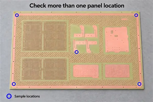
For a registration investigation, record the panel, sample location, layer pair, datum and measurement direction. A microsection through one hole provides local evidence; it doesn’t establish the condition of every hole on a panel. Likewise, a continuity pass can coexist with a reduced annular-ring margin. Electrical and geometric results answer separate questions.
Design and review for usable margin
Registration risk is easier to manage while pad and clearance geometry can still change. Review capture pads and antipad clearances against the specified drill requirements, not just the finished-hole size. Keep artwork, drill data, layer order and stack-up revisions consistent. Examine narrow clearances and small capture pads early in design for manufacturing review, and agree on controlled features and inspection criteria before tooling is finalized. Recheck margins if the material, panel arrangement, via construction or bonding sequence changes.
For high-density structures, small capture features and sequential build-up make registration especially consequential. A stated fine-line capability doesn’t by itself specify how accurately layers can be positioned. Impedance-controlled designs also need review of their actual conductor geometry: a shift between broadside-coupled traces can affect overlap differently from a shift over a wide, continuous reference plane.
Useful data for a fabrication review includes the complete fabrication package, layer order, proposed stack-up, drill information and drawing tolerances. For a specific registration requirement, identify the affected layers or vias, intended datum, acceptance criteria and requested inspection records. If a prior lot showed an offset, measured coordinates and sample locations are more useful than an unscaled photograph. The agreed requirement should state both the construction and the inspection scope, since a generic capability value doesn’t define the tolerance for every layer pair.
Questions engineers ask
Are assembly fiducials the same as inner-layer targets?
No. Assembly fiducials help locate the board or component region for placement equipment. Inner-layer targets support fabrication alignment or measurement. Their roles and stages differ, even if both use recognizable copper shapes.
Can a board pass electrical testing with poor registration?
Yes. A connection can remain continuous with less annular-ring margin than intended. Electrical results don’t replace geometric acceptance checks.
Can registration be checked after assembly?
Some internal features may be visible with suitable X-ray equipment, though components, shields and overlapping copper can complicate interpretation. Fabrication targets, coupons and production-stage records are often more useful for investigating a specific layer-pair offset.
Will a larger pad always solve misregistration?
No. More pad area can improve hole capture, but it may reduce spacing to neighboring copper or change routing and electrical behavior. Review both connection margin and isolation clearance while investigating the source of the offset.
The useful output of a registration review is a defined measurement tied to the actual board geometry: which features are compared, from what datum, at what stage, and against what acceptance criterion. That gives design and fabrication teams a shared basis for judging whether the available copper and clearance margins remain adequate.