PCB Tombstoning: Causes, Inspection and Process Controls
- li
- 923 reads
Uneven wetting can lift a chip component during reflow. Paired checks of pads, paste, placement and temperature help pinpoint the cause.

A chip component that stands on one end has lost a connection, but its appearance alone won’t reveal why. PCB tombstoning occurs when unequal soldering forces rotate a two-terminal component during reflow. The practical task is to find what made the two joints behave differently: pad and copper geometry, paste deposits, placement, component condition or heating history.

Start the investigation at the affected reference designator. Compare its two joints and the conditions immediately before reflow, then check the same component at a known-good location. A profile adjustment on its own may hide a symptom while leaving the cause in place.
What happens when a chip tombstones?
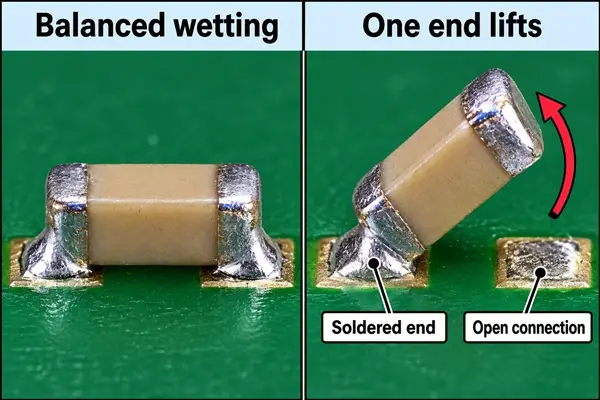
During reflow, molten solder wets the component terminations and the board pads. If one joint wets first, or if the forces acting at the two ends differ, the component can rotate and lift away from one pad. The other end may remain attached, leaving an open connection at the lifted termination.
A component can stand nearly upright or rise only partway. Both conditions matter: partial lift can also interrupt electrical contact. “Manhattan effect” and “drawbridge effect” describe similar appearances. A chip shifted sideways is a different defect; inspect the orientation and both terminations before classifying it.
The circuit determines the functional consequence. An open series resistor can break a signal path. A disconnected bypass capacitor may still allow the product to power on while reducing the intended decoupling. A functional check should therefore reflect what the affected component does.
Small packages need closer process control
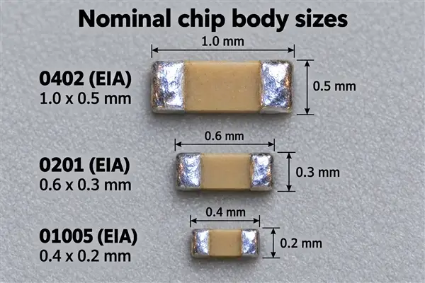
Small chip resistors and ceramic capacitors are common candidates because their low mass gives an imbalance less resistance to rotation. Packages such as 0201 and 0402 warrant close attention to paste printing and placement overlap. Package names need their sizing convention: an imperial 0402 is not the same size as a metric 0402.
| Imperial / EIA designation | Metric designation | Nominal body length × width | Assembly consideration |
|---|---|---|---|
| 0402 | 1005 | 1.0 × 0.5 mm | Check termination overlap and copper connections at both ends. |
| 0201 | 0603 | 0.6 × 0.3 mm | Small printing or placement differences can become significant. |
| 01005 | 0402 | 0.4 × 0.2 mm | Confirm package-specific printing, placement and inspection capability. |
These are nominal body dimensions, not pad dimensions or acceptance tolerances. Use the exact component drawing for body height, termination length and recommended footprint. A resistor and capacitor with the same nominal package can behave differently because their termination construction and solderability may differ. Other two-terminal parts can also lift, so diagnose the actual component rather than assuming every case involves a capacitor.
Check pads and copper before changing the oven
Compare each pad’s length, width, spacing and exposed solderable area with the component manufacturer’s recommended land pattern. Oversized or asymmetric pads can change solder shape and the forces on the terminations. Reducing pad dimensions without checking attachment requirements may replace a tombstone problem with an inadequate joint.
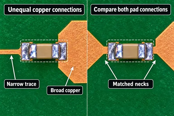
Then trace the copper connected to each pad. One end tied to a broad plane and the other connected through a narrow trace may heat differently. Internal copper, nearby vias and surrounding components can also affect the local thermal response. A recurring lifted end beside a copper plane makes that area worth investigating; it does not by itself establish the plane as the cause.
Matched copper connections or thermal reliefs may reduce a difference, but must still meet current capacity, grounding and signal needs. An unfilled via near a solderable pad can also affect solder volume. Review the pad, solder-mask opening, copper and via treatment together before changing the layout.
Compare the two printed deposits
Unequal solder paste can leave one termination higher or in contact with less paste before melting. Differences in solder volume may also change the forces at the ends of the component. Check the two deposits’ volume, height and position individually; a board-wide average can conceal a local mismatch.
Potential contributors include blocked stencil apertures, registration error, contamination on the stencil underside and inconsistent paste release. A symmetric aperture design doesn’t guarantee that the printed deposits will be symmetric. An SMT stencil needs to suit the package and board, and the resulting print should be checked on the assembly.
If measurements identify excess paste at the outer ends of a chip as a contributor, a controlled aperture change may be useful. A universal reduction isn’t appropriate for every package. Verify the resulting joints, attachment and print repeatability, and watch for opens or poor wetting elsewhere.
Verify placement and thermal history
Offset or skew can give the two terminations unequal overlap with their paste deposits. A placement-height error can leave one end without proper contact even when the image appears centered. Check package definitions, nozzle condition, pickup, board support and placement settings at the affected reference designators.
Don’t rely on solder self-alignment to correct a component placed beyond its process tolerance. Increasing placement force without checking component limits can damage a ceramic body or displace paste. When available, retain the pre-reflow image; it can help distinguish an initial placement error from rotation during melting.
Measure the temperature history at the assembly before changing the oven recipe. Zone setpoints don’t show the temperatures reached at the two joints. Compare the affected area with a stable location and assess whether the joints approached melting at different times. Small chips can be difficult to measure because sensor size and attachment may disturb the reading, so use a consistent method and a suitable instrumented board.
Preheat or soak adjustments may reduce temperature differences, but excessive exposure can deplete flux activity or exceed a material’s recommended limits. Keep the measured profile within the solder paste window and component limits. Raising the peak can’t correct a poor footprint or unequal paste deposits.
Changes to atmosphere or alloy also need controlled trials. Nitrogen can accelerate wetting and may worsen an existing imbalance; it isn’t an automatic fix. Switching to air can affect other joints. Judge the full assembly result, not only the lifted component.
Record paired measurements
Use measurements from the affected component alongside a known-good position or build. Numerical limits must come from the selected component, paste and qualified assembly process; a generic checklist cannot set production acceptance criteria.
| Parameter | Unit or calculation | What to record | How to use it |
|---|---|---|---|
| Body and termination dimensions | mm | Part number, package convention, body and termination dimensions | Confirm the land pattern and placement definition. |
| Pad and mask geometry | mm; mm² | Length, width, gap and exposed area at both ends | Compare the drawing with the exposed pads. |
| Stencil aperture and thickness | mm or µm | Aperture dimensions, shape, foil thickness and revision | Review deposit design and local release behavior. |
| Printed paste volume | mm³ | V1 and V2 for the paired pads | Compare individual deposits, not just a board average. |
| Relative volume difference | 100 × |V1 − V2| / [(V1 + V2) / 2] | Percentage and original volumes | Compare trials consistently; this is not a pass/fail limit. |
| Paste height and position | µm; X/Y offset in mm | Both deposits and their positions relative to the pads | Identify unequal seating or print registration. |
| Placement | X/Y in mm; rotation in degrees | Offset, skew and approved Z-height or force settings | Check overlap before reflow. |
| Temperature history | °C and seconds | Measurement locations, preheat, peak and time above the alloy’s liquidus | Compare the board profile with material limits. |
| Heating rate | °C/s | Temperature interval and measurement method | Assess changes without treating zone settings as board temperature. |
| Defect frequency | Defective components / inspected opportunities | Reference designator, panel position, lot and trial size | Check whether a change improved repeatability. |
For example, illustrative volumes of 0.008 and 0.010 mm³ produce a relative difference of 22.2% using the formula above. That figure quantifies the mismatch; it doesn’t define an acceptable production limit. Keep the absolute volumes and measurement settings with the percentage so later trials can be compared consistently.
Trace recurring defects to a cause
Look at where the defects occur. Repeated failures at one reference designator call for a different line of inquiry from scattered failures across identical components. A pattern at one panel edge may point toward support, printing or heating conditions. A change that coincides with a new component reel, paste lot or stencil revision provides another testable lead.
- Preserve the evidence. Record the lifted end, board orientation, reference designator and lot before rework.
- Check the pre-reflow state. Compare paired solder-paste inspection measurements and placement images.
- Review the design. Inspect pad geometry, copper connections, vias and the component drawing.
- Check materials and heat. Review paste handling, termination condition and measured profile.
- Run a controlled trial. Change one identified factor and record the other settings, sample size and defect count.
- Inspect the whole board. Check for bridging, insufficient solder and other defects alongside any reduction in tombstones.
Automated optical inspection can flag component position and visible joint abnormalities. Microscope review helps confirm the physical condition. Electrical testing establishes circuit behavior, but doesn’t show whether printing, placement or heating caused the defect. The investigation needs these records together; neither one image nor a passing functional test identifies the root cause.
Tell tombstoning apart from other solder defects
| Condition | Physical distinction | Likely electrical concern | Inspection focus |
|---|---|---|---|
| Tombstoning | One end of a chip lifts from its intended pad | Open connection or loss of the component’s function | Orientation and attachment at both terminations |
| Solder bridging | Solder joins conductors that should remain separate | Unwanted short circuit | Clearance and continuity between adjacent nets |
| Poorly formed or cold joint | A joint fails to form properly; the component need not stand upright | Open, high-resistance or unstable connection | Wetting, joint integrity and process history |
| Billboarding | A chip rolls onto its narrow side | Depends on termination contact and assembly requirements | Body orientation and specified mounting condition |
| Solder graping | Fine solder particles remain uncoalesced around a deposit | Joint-quality concern distinct from chip rotation | Particle coalescence and the surrounding joint |
A solder bridge is not another name for a tombstone, though multiple defect types can appear on one board. A dull lead-free joint alone doesn’t establish cold soldering, and a chip standing upright doesn’t prove that the reflow peak was too low.
Rework the component and verify the repair
Use an approved rework method suited to the component and PCB. Isolate the board from power, follow ESD controls and inspect the chip, pads and nearby parts. A cracked body, damaged termination or lifted pad needs assessment; pressing the component flat doesn’t resolve that damage.
For a reusable component, rework must release it without force against solid solder, restore a suitable solder amount and position both ends correctly. Replace the part if its integrity is uncertain or assembly requirements call for it. Heating tools, preheat and exposure limits depend on the package and board.
After rework, inspect both joints and check the relevant electrical function. Record the location and any required cleaning or retest. A successful repair addresses that board; it doesn’t demonstrate that the production cause has been removed. Verify the next build with a corrective-action trial.
Use process records to close the loop
PCB assembly can be reviewed across design for assembly, stencil fabrication, paste printing, 3D solder-paste inspection, placement, reflow, optical inspection and functional testing. Each stage supplies different evidence: paste inspection checks the deposits, placement review checks the chip before melting, and post-reflow inspection checks the completed attachment.
For example, the available equipment includes a SINIC-TEK S8080 3D solder-paste inspection system and a SINIC-TEK A510DL 3D optical inspection system. Equipment readings need to be judged against the project’s component requirements and agreed acceptance criteria.
For a board review, useful records include PCB files, a bill of materials with exact manufacturer part numbers, placement data and the assembly drawing. For an existing defect, add clear photographs, affected reference designators, failure counts and available printing or profile data. Those details help focus the investigation on a measurable difference between the two ends of the component.
Common questions
Can a board with a tombstoned capacitor still power on?
Yes. A disconnected decoupling capacitor may not prevent startup, though the circuit has lost part of its intended filtering. Powering on alone doesn’t establish that the assembly meets its requirements.
Does lead-free solder always cause more tombstoning?
No. The alloy’s melting behavior, paste formulation and imbalance between the two joints all matter. Treat each alloy and process as a specific combination; changing alloy won’t necessarily resolve a footprint problem.
Should every tombstone be blamed on the assembly operator?
No. Design geometry, component condition, paste printing, placement and thermal history can all contribute. Preserve the evidence and identify the process contribution before assigning corrective action.
The useful next step is a paired comparison: measure both pads, deposits and placement, then relate those findings to the local thermal history. That turns a visible defect into a testable process question and gives each corrective change a result to verify.