Mixed Surface Finish PCBs: Specifying Contacts, Solder Pads and Process Boundaries
- li
- 970 reads
Mixed finishes pair wear-resistant contacts with solderable pads. Clear region maps, deposit limits and inspection criteria help prevent process and assembly problems.
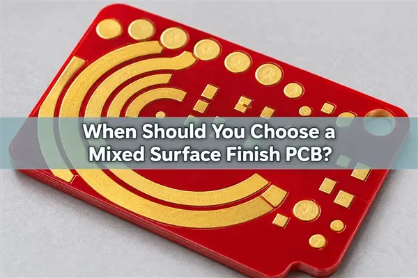
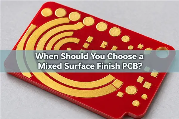
A mixed surface finish PCB gives different exposed copper areas different finishes. The practical case is straightforward: a connector that mates repeatedly may need a wear-resistant hard gold deposit, while component pads need a surface suited to soldering. Assigning each region its own finish can meet both requirements, but it adds process and inspection details that a single-finish board does not need.
The choice starts with the job each area must perform. A finish name alone does not define that job. The drawing and specification need to show where each finish goes, what deposit stack and thickness are required, and how the completed regions will be checked.
Separate contact duty from soldering duty
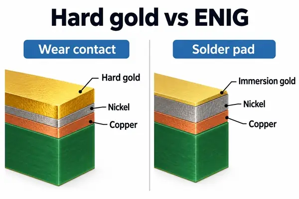
Contacts and solder pads experience different conditions. Mating or sliding contacts face repeated mechanical wear, so their surface must suit the required contact system and service life. Solder pads need a surface compatible with the assembly process, including solder wetting and the flatness required for component placement.
Hard gold is used for contacts that need a specified wear-resistant coating. ENIG, or electroless nickel immersion gold, is commonly used for solder pads where a flat surface is useful. Its thin gold cap dissolves into the solder during reflow; it does not provide the same wear surface as a hard gold contact deposit. Conversely, applying thick hard gold to solder pads introduces gold into joints that may not have been qualified for it.
The distinction matters even when both regions look gold-colored. Color cannot establish which process was used or confirm the deposit thickness. The functional requirements and the finish stack must be documented separately.
Fine-pitch packages can make pad flatness a significant assembly consideration. That does not make ENIG mandatory for every HDI board: package geometry, finish choice and assembly process need to be compatible. A high-density interconnect board still needs a finish selected for its actual pads and contact areas.
Choose combinations for defined functions
Common pairings include hard gold with ENIG, hard gold with lead-free HASL, hard gold with immersion silver, and selective ENIG with OSP. These are possible process routes, not interchangeable recipes. The intended regional functions, layout, protection steps and process order determine whether a particular combination is suitable.
| Combination | Typical regional use | Points to resolve |
|---|---|---|
| Hard gold + ENIG | Wear contacts and flat solder pads | Separate deposit requirements, contact protection and plating access |
| Hard gold + lead-free HASL | Wear contacts and solder-coated pads | Pad planarity, heat exposure and protection of contacts |
| Hard gold + immersion silver | Wear contacts and flat solderable areas | Handling, packaging and protection against contamination or tarnishing |
| ENIG + OSP | Selected nickel/gold areas and OSP-protected solder pads | Selective coverage and compatibility between process chemistries |
Immersion tin and ENEPIG are other finish options, but adding another finish has to solve a defined functional need and have a suitable manufacturing route. ENEPIG is a nickel, palladium and gold stack on a region; multiple layers in one stack do not by themselves make the board a mixed-finish design.
A single finish is usually the simpler choice when it meets every exposed area’s needs. A mixed finish earns its added masking, sequencing and verification work when one finish would compromise either contact wear or assembly performance. For a board whose exposed pads are all soldered and have no special contact or bonding function, a second finish may add cost without resolving a real requirement.
Define regions on the fabrication drawing
Provide a dedicated finish drawing or clearly named fabrication layers. Mark each region, its finish and its boundary, and state the default finish for exposed pads outside the marked areas. The finish map must agree with the copper and solder-mask data.
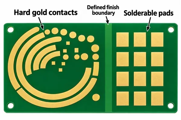
- Identify the board revision, side and region names, such as contact region A and solder-pad region B.
- Specify the full finish stack in each region, including a nickel underplate where required.
- Mark test pads, plated holes and any areas that must not receive a particular deposit.
- Dimension boundaries and nearby features from an agreed datum. Do not rely on colors in a PDF alone.
- Show how a boundary may approach a solder-mask opening or contact wear track.
Solder-mask openings identify exposed copper; they do not, by themselves, tell the fabricator which plating operation applies. Through-holes and shared exposed features can also complicate attempts to give the two board sides different finishes. For a rigid-flex board, identify the rigid and flexible regions so the contact geometry and masking access can be assessed against the actual construction.
Plan the process sequence and electrical access
Manufacturing combines surface preparation with selective exposure or protection, followed by the specified finish operations and regional inspection. The sequence depends on the chosen combination; it needs review for the actual board rather than being treated as a universal recipe.
- Check the finish map, board materials, exposed features and acceptance requirements against the fabrication data.
- Plan electrical access for electrolytic plating and protect areas that must not receive that deposit.
- Apply the contact finish using the selected preparation and masking route.
- Process the other regions while protecting completed areas from incompatible chemistry or heat.
- Complete profiling and contact-edge operations, then verify coverage and coating requirements by region.
Electrolytic hard gold needs an electrical current path during plating. Isolated or staggered contacts may therefore need temporary plating connections, which are removed or isolated in the finished board. ENIG deposition does not require that external electrical bus connection. That difference can affect routing and tooling decisions before fabrication data is released.
Specify thickness and assembly conditions by region
State thickness requirements separately for each deposit and region, with units and acceptance limits. Copper, nickel and gold are distinct layers; a single “plating thickness” value does not define their individual requirements. Geometry, contact wear and assembly exposure also need their own specifications.
| Parameter | Specification detail |
|---|---|
| Hard gold | Deposit type, contact region and minimum or range. A stated capability reaches 50 microinches (1.27 micrometers), subject to design review; this is not an automatic default. |
| Nickel underplate | Separate thickness range and the region where it applies, in micrometers or microinches. |
| ENIG region | Individual nickel and gold layer limits, with the applicable finish specification and revision. |
| Finish boundary | Position, tolerance and permitted proximity to openings, dimensioned in millimeters from a drawing datum. |
| Contact engagement | Usable contact length, edge profile, bevel angle where applicable, and required mating cycles. |
| Assembly exposure | Solder alloy, planned thermal passes, cleaning chemistry and relevant process conditions. |
| Thickness verification | Layer model, measurement sites and lot or coupon identification for each deposit and region. |
For reference, 1 microinch equals 0.0254 micrometers; 30 microinches equals 0.762 micrometers, and 50 microinches equals 1.27 micrometers. Those conversions help avoid unit errors, but they do not select a suitable contact coating. Contact force, wear path, mating surface and required life determine the requirement.
Assembly and storage conditions need to suit every finish on the board, including contacts that will not be soldered. OSP protects copper until soldering, so handling and accumulated heat exposure matter. Immersion silver needs protection from tarnishing and contamination. HASL leaves a solder coating whose planarity must suit the component pads. ENIG provides a flat solderable region, but it does not make the assembly immune to contamination or process damage.
Identify finish details alongside the bill of materials and assembly drawing when boards will be assembled. Keep solder paste and flux away from unsoldered wear contacts, and check compatibility with cleaning and any later coating operation. Use the approved packaging and process conditions for the full combination; storage assumptions for one finish do not establish the shelf life of a mixed-finish board.
Inspect each finish where it is applied
Inspection should follow the finish map and verify both coating requirements and functional needs. A thickness reading from one accessible pad cannot represent several separately processed regions.
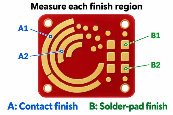
- Coverage: Check that each specified pad has the correct treatment and that boundaries match the drawing.
- Thickness: Use an appropriate calibrated method, such as X-ray fluorescence with the correct coating-stack model, at agreed locations.
- Surface condition: Apply the specified deposit checks and look for damage, residue or exposed areas.
- Solderability: Assess the solder-pad finish under the required conditions; a contact wear test does not answer this question.
- Contact performance: Test mating or sliding duty with the actual contact system and its electrical acceptance criteria.
Continuity testing checks the circuit; it does not establish plating thickness, solderability or wear life. Keep the board revision, inspection locations and lot information linked to the results. If a defect appears after assembly, compare retained bare-board evidence with assembly history before assigning a cause.
Boundary defects can include unwanted coverage, exposed copper, residue or damage from a later process. A transition should not cross an active wear track or joint area unless that arrangement has been designed and qualified. Closely spaced pads may leave too little room for selective protection, so the actual geometry needs review rather than a clearance rule copied from another process. A clean-looking gold surface also cannot prove the nickel beneath it is sound; discoloration should be investigated rather than judged by color alone.
Evaluate cost and prepare a quotation
Selective plating can reduce the area receiving an expensive deposit, but the finished board is not automatically cheaper. Added masking, tooling, handling and verification may outweigh the material savings, particularly on a small prototype run.
Compare complete-board costs at the same quantity, panelization, thickness requirements, finished area and inspection scope. The single-finish alternative must meet the board’s actual requirements: an all-ENIG quote is not equivalent if the contact needs qualified hard gold. Include expected repeat demand so one-time preparation can be distinguished from recurring process costs.
A useful quotation package brings together the fabrication data, finish map and performance requirements. Include Gerber or equivalent data, drill files, stack-up and board dimensions; identify both sides, defaults, exceptions and thickness requirements; and provide connector drawings, wear or mating requirements, bevel details and restrictions on temporary plating connections. For assembled boards, include the bill of materials and soldering and cleaning conditions. Quantity, acceptance criteria, inspection records and delivery requirements complete the request.
The most useful design decision is to tie every finish region to a specific job, then make the drawing, thickness limits, process sequence and inspection plan agree. That gives the fabricator enough information to assess selective plating before the purchase specification is finalized—and gives the assembly team clear requirements for both the solder pads and the contacts.